Vertically Integrated Capabilities
Sensor Manufacturing
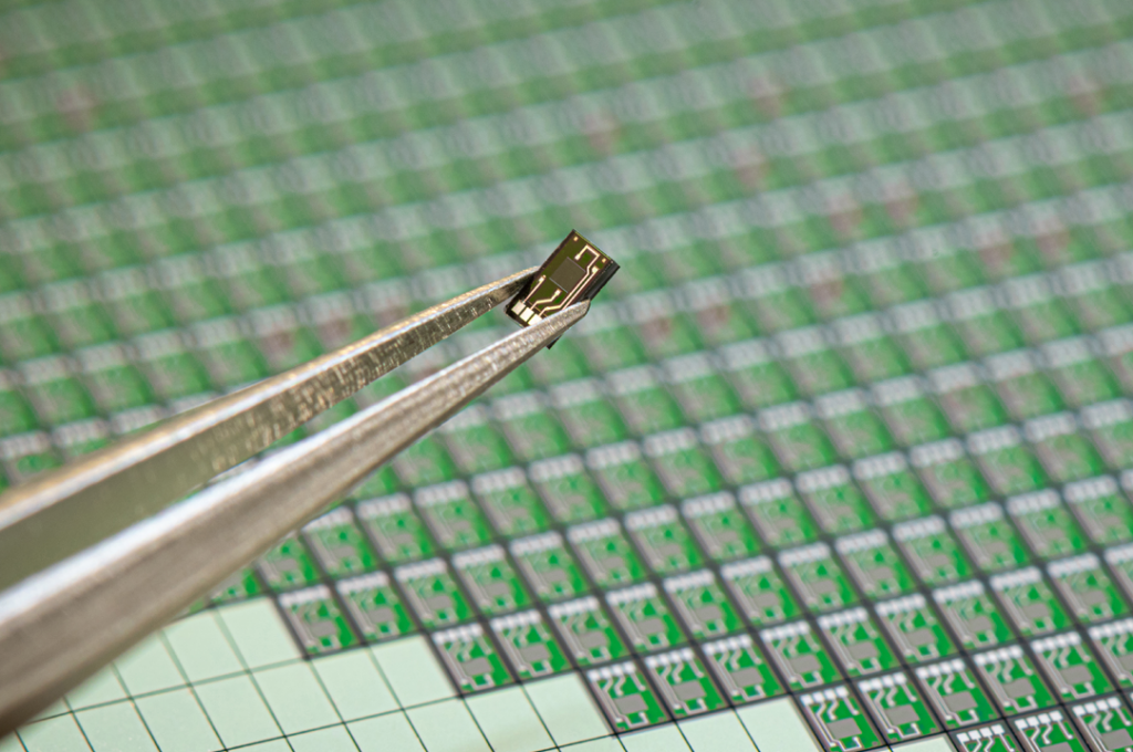
At our inhouse semi-conductor production facility, we have many years of experience in developing and producing high quality miniature sensors. We perform the lithography and chemical vapor deposition ourselves, as well as the diffusion and annealing furnaces. After testing the wafers, they are diced and picked by well-trained special operators.
Our portfolio contains various dimensions of ISFET pH sensors and Wheatstone full bridge pressure sensors. And more sensors will follow.
Product Development
Sentron is your partner for the full process: starting with semiconductor processing to documentation required for the MDR. Anything is possible, depending on the preferences of the customer.
At the start of the partnership, we will discuss which processes the customer would like Sentron to do. This can vary between the bare sensor die to a full sensor product with GUI.
During the prototyping phase the sensor module design can be changed and concepts can be tested. After the engineering project has been finalized, Sentron offers standardized volume assembly of the sensor. The sensor component is subsequently assembled into the end product by the customers.
Sensor Integration
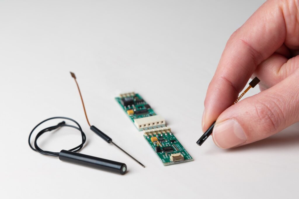
Sentron has specific know-how in die attaching, wire-bonding, encapsulating, steering and compensating the sensor. We can provide successful R&D engineering services for any sensor integration into your product. This contract development and manufacturing of sensor assemblies is feasible for any shape or dimension and for any kind of product and application.
Processes required for the pH prototypes include the placement of our pH ISFET sensor on the PCB after which it will be wire-bonded, glob-topped and encapsulated. The reference electrode has to be designed such that it fits into the assembly. A diaphragm is placed in the reference chamber wall and the chamber will be gel filled. For the pressure sensor prototypes the outline is similar. However, this sensor does not require a reference electrode.
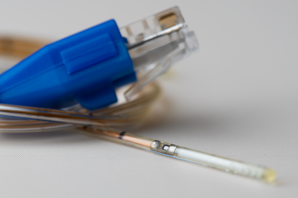
The design of the electronics that is required for the steering of the sensor is included, as well as the custom-made housing for the assembly. Finally, a cable is attached, if required.
Extensive Facilities
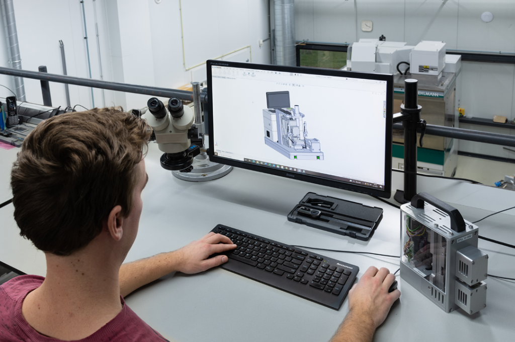
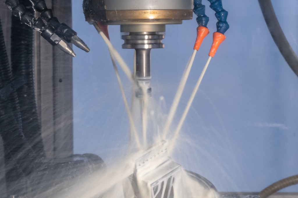
We have all the necessary equipment in place at our Leek facility, including a semi-conductor production and testing factory, a fully equipped tooling shop (including a 5-axel CNC milling machine), an electronic and PCB circuit design facility, a software development unit and a fully equipped sensor and product assembly facility.
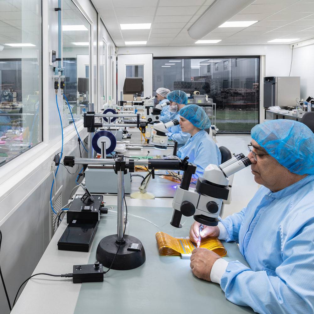
We have a clean room facility for development, manufacturing, product testing, and qualification services of sensors, assemblies and meters. These are necessary for the determination of physical and chemical values measured in the engineering field.
Certifications
